FAB

FABrIC Logo white

Teledyne Micralyne Micralyne MicraGEM-Si™ MEMS Process

Teledyne Micralyne logo

Description

Micralyne MicraGEM-SiTM is a silicon-on-insulator (SOI) based MEMS process which will reduce the initial cost and risk of prototype development, while speeding the time to market for MEMS- Based devices.

MicraGEM-SiTM is ideally suited for the manufacture of tilting mirrors and mirror arrays for variable optical attenuators (VOA) and wavelength selective switch (WSS) modules, commonly used in fiber optic telecom networks as well as resonators, inertial and bio sensors.
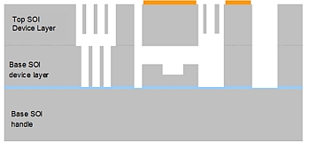


Note: The expected number of chips to be delivered for this technology is 15.

Applications

  • Display technology
  • Optics and telecommunications
  • Inertial sensing
  • Biomedical and environmental sensing

Sevices

  • Design kits
  • Documentation including design handbooks
  • Datasheets can be ordered from http://www.micralyne.com/data-sheets/
  • Design rule checking services
  • CMC engineering support
  • Access community-based support and collaborations
  • Design consultation*
  • Packaging & assembly services*

* Additional charges apply.
Features

  • Two thick SOI structure layers with up to three functional levels of silicon thickness option. This enables structures such as vertical comb-drive actuators.
  • Base and top device layers are electrically connected through the bond interface, allowing 3D routing of electrical signals.
  • Patterned low-stress gold metallization on the top surface is suited for highly reflective mirrors and contact pads for gold wire bonding.
  • Design size 4 mm x 4 mm
  • SOI MEMS
  • Two structure layers
  • Three trench depths

Design Kits and Libraries

Pricing

List Price
Price for Subscribers

Dedicated runs only. Contact fab@cmc.ca.

Dedicated runs only. Contact fab@cmc.ca.

Licensing

Contact licensing@cmc.ca.

Minimum Access Requirement

For Canadian Academics

Does your research benefit from products and services provided by CMC Microsystems?

FABrIC Challenges

Stimulating innovation in semiconductor fabrication processes for product development

Scroll to Top
Skip to content